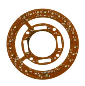
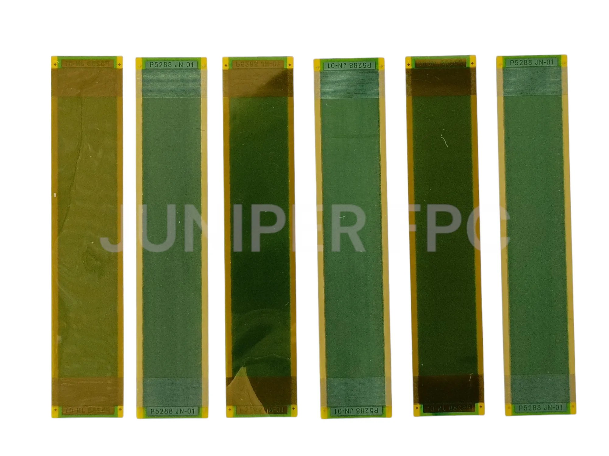
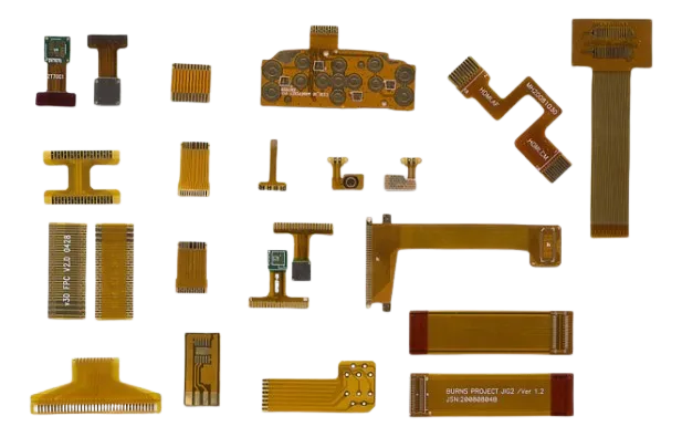
Single-sided Flex PCBs / Flex Circuits
Double-sided Flex PCBs / Flex Circuits
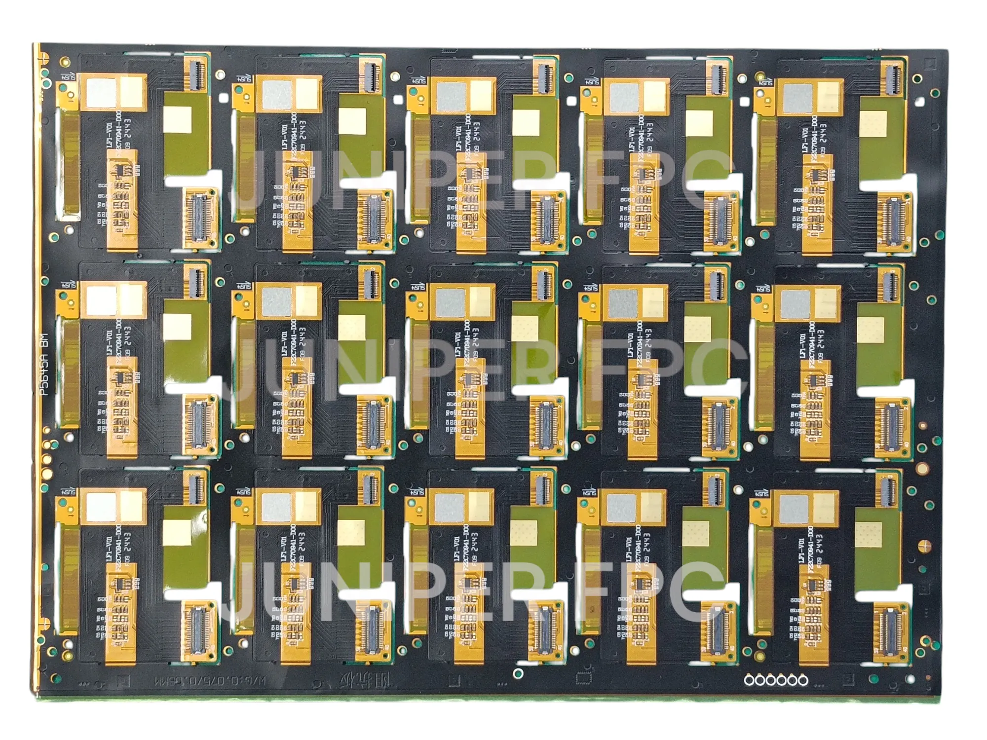
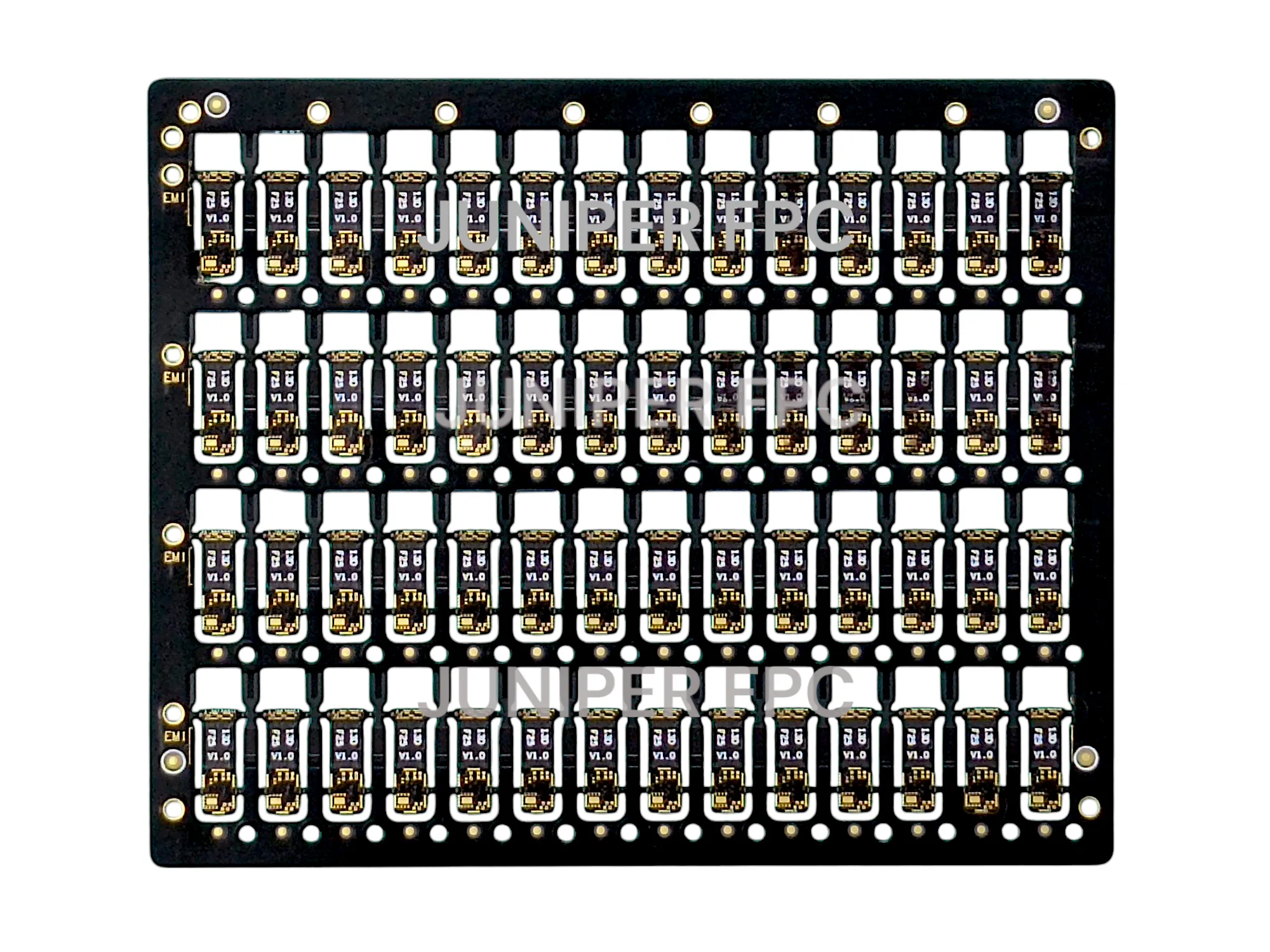
Multilayer Flex PCBs / Flex Circuits
HDI Flex PCBs / Flex Circuits
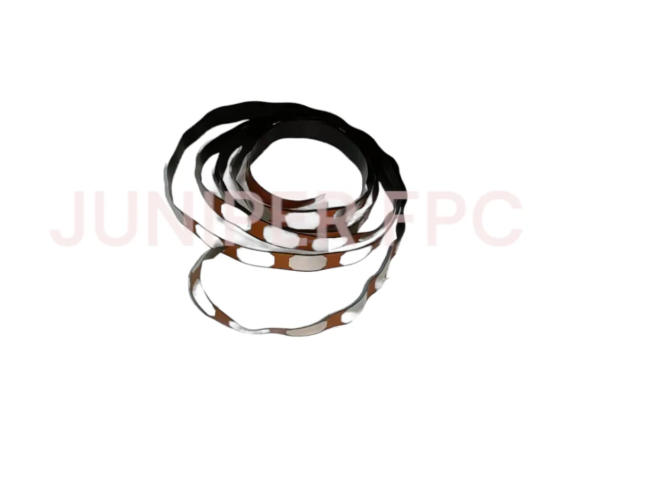
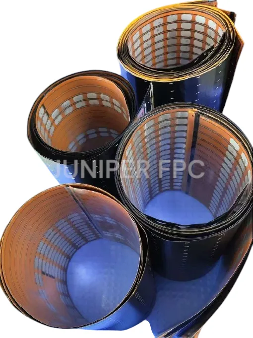
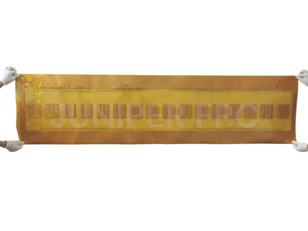
Ultra-long Flex PCBs / Flex Circuits
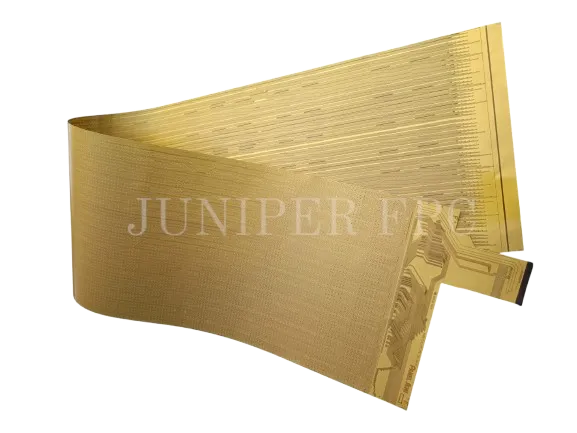
Ultra-thin Flex PCBs / Flex Circuits
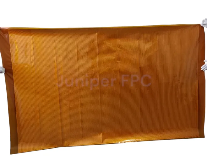
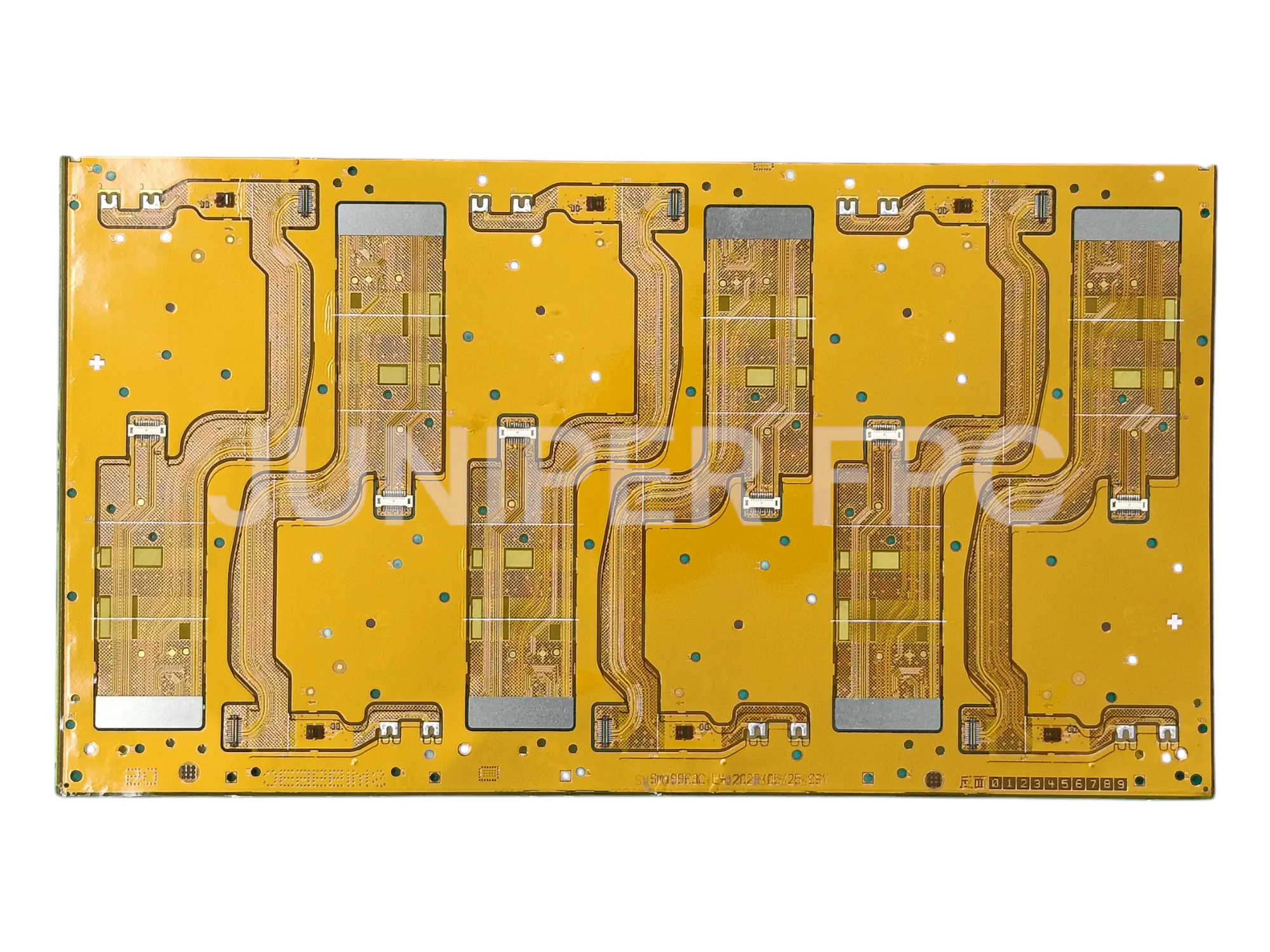
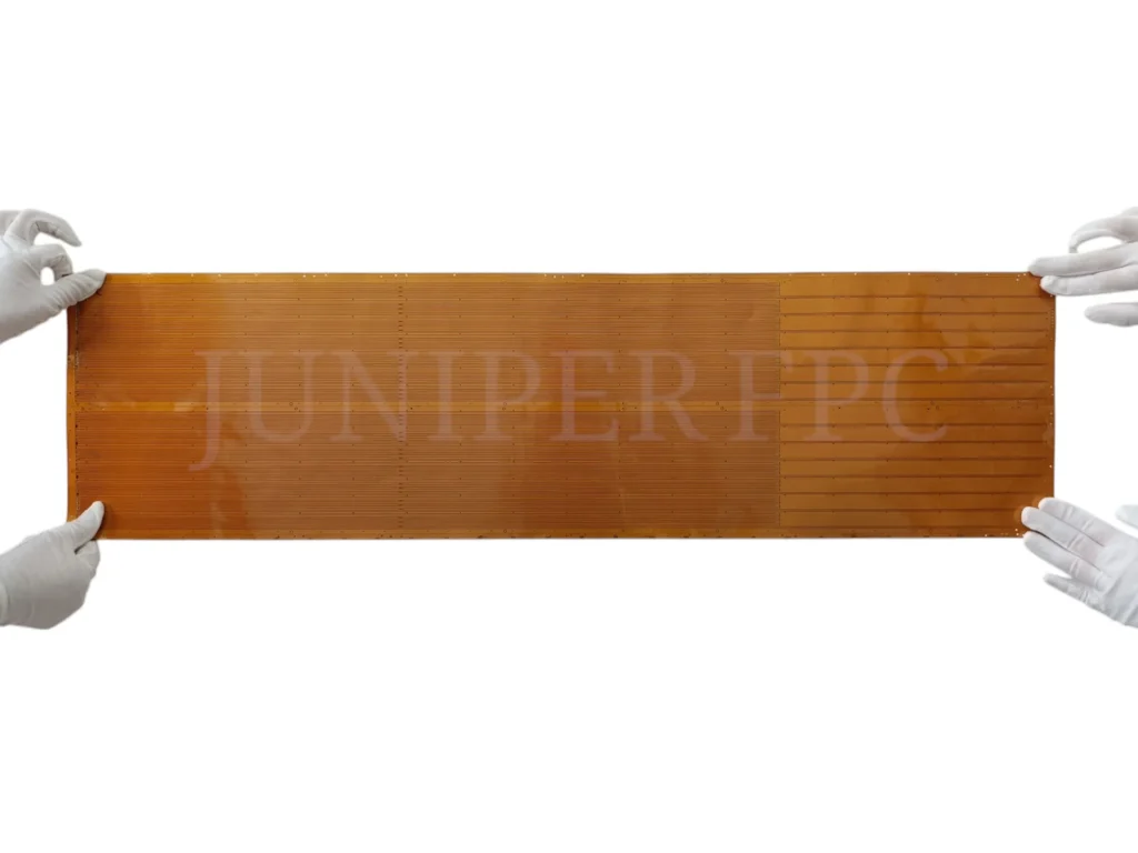
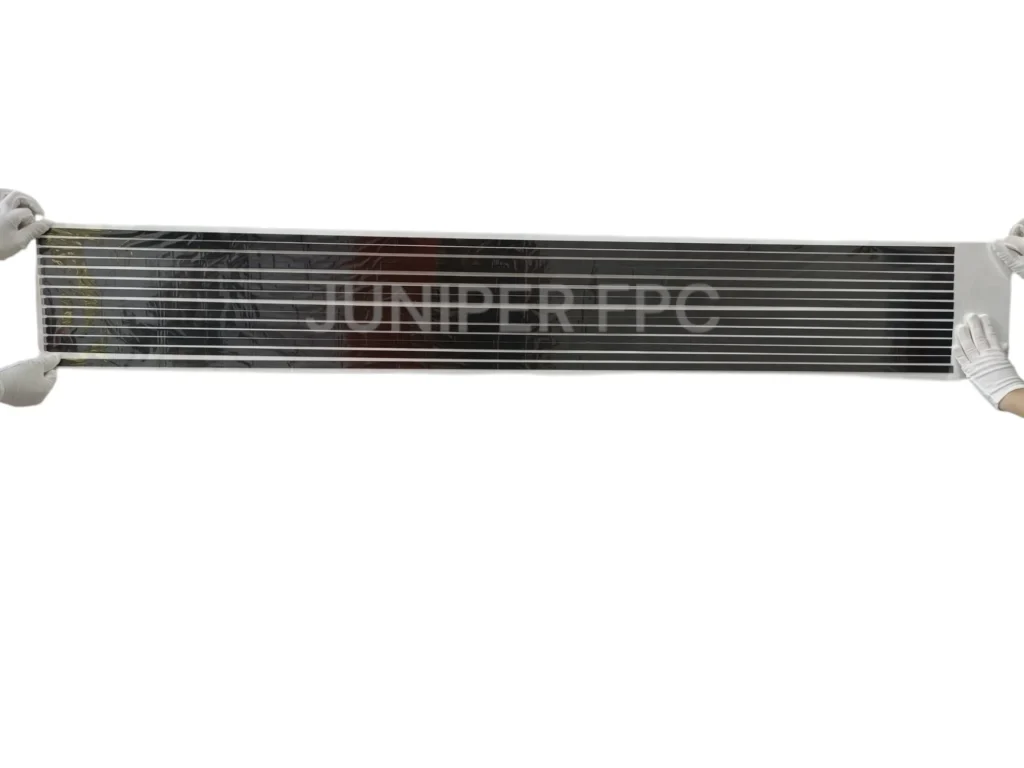
Large Size Flex PCBs / Flex Circuits
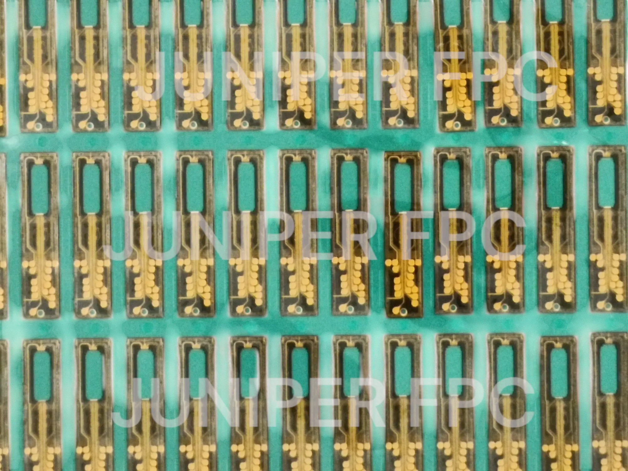
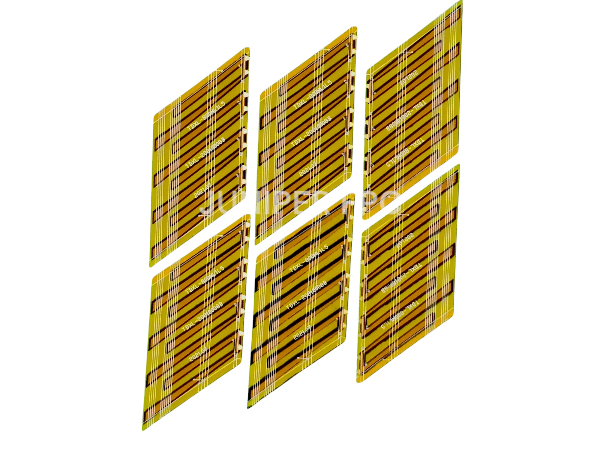
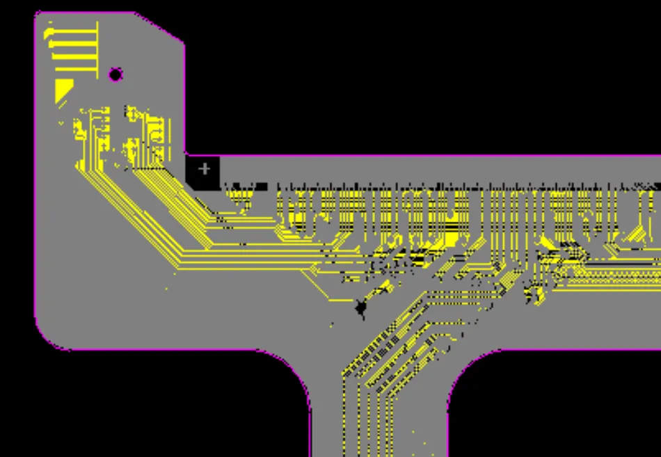
Ultra Fine Line Flex PCBs / Flex Circuits

Custom Flex PCBs / Flex Circuits


Consumer Electronics

Automotive

Medical Devices

Aerospace

Industrial Equipment

Telecommunications