Rigid-flex PCBs combine the benefits of both rigid and flexible boards, but they come with unique challenges.
Designing rigid-flex PCBs can be tricky, with multiple challenges including material selection, layer stack-up, and thermal management.
These complexities demand a keen understanding of design guidelines and the right strategies to ensure reliability and performance. If the design is not good, there will be troubles during manufacturing and the use of the products.
1. Understanding the Basics of Rigid-Flex PCBs
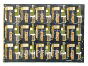
Rigid-flex PCBs are commonly used in aerospace, medical, and industrial control industries. Flexi rigid PCBs are a combination of rigid and flexible circuits, designed to offer both mechanical strength (for stability )and flexibility (for bendability ). Understanding their basic structure is the first step in addressing design challenges.
Rigid-flex PCBs are commonly used in applications where space is limited. These boards offer significant advantages in reducing size, improving performance, and enhancing reliability.
- Rigid Sections: Standard PCB materials, typically FR4 or high-performance materials. Try to use FR4 to save the costs of the product. The rigid part provides strength, durability, and ease of mounting components.
- Flexible Sections: The flexible areas are made from flexible substrates, typically polyimide or other flexible materials. Some suppliers offer a wide variety of RF PCB materials. If you have a choice, it is better to choose the most common type of FR PCB material because the delivery time is shorter and more cost-effective.
- Layer Count: 2 to 4 Layers,6 to 10 Layers,10 to 18 Layers, different layer stages meet the different requests from low to high function of the end products. The layers must be an even number. The flexible section must be in the center/middle of the PCB.
- Surface Finish and Surface Effects: HASL (Hot Air Solder Leveling), ENIG (Electroless Nickel Immersion Gold), OSP (Organic Solder Ability Preservative). ENIG is a standard surface finish.
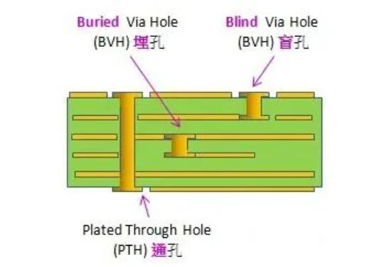
- Via Types and Placement: Three types of vias designs for different usages. Through-hole Vias go through the entire PCB, providing electrical connections from the top to the bottom layers. Commonly used in rigid sessions (FR4), but also could be used in flex sessions with the proper placement to avoid stress during bend. Blind Vias connect inner layers to the outer layer but do not go all the way through the PCB. It is located on the top and bottom surfaces of printed circuit boards. They have a certain depth and are used to connect the surface circuits to the inner circuits below. The depth of the holes usually does not exceed a certain ratio (aperture). Buried Vias are internal vias that connect layers within the board but do not reach the outer layers. They are used for high-density routing and to avoid interference with surface-mounted components.
2. Material Selection Challenges
Choosing the right materials for a rigid-flex PCB is a critical step that impacts both performance and manufacturing costs. Material thermal conductivity, flexibility and durability need to be considered carefully.
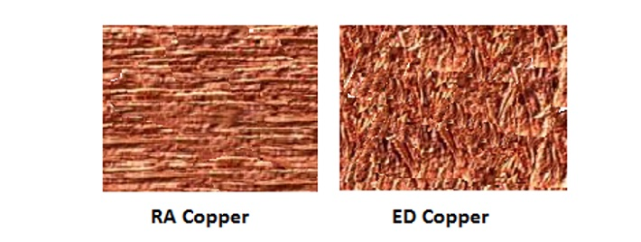
Polyimide (PI) and FR4 are commonly as the first consideration at the beginning of rigid-flex PCB design, each offering distinct advantages and trade-offs in terms of flexibility, thermal resistance, and durability.
Polyimide has excellent thermal stability, while FR4 has the ability to support the structure of flexi rigid PCBs. The challenge lies in balancing cost, performance, and manufacturability to ensure the PCB meets both design specifications and budget constraints. Comprehensively consider the operating frequency and signal transmission speed of the circuit; the high heat resistance, corrosion resistance, mechanical strength, processing performance and cost factors of the material to find the most suitable material to meet the needs of the product. Therefore, understanding the usage scenarios of the product will help Juniper FPC give you better suggestions on material selection.
3. Defining the Stack
Defining the stack by area involves tailoring the number and arrangement of layers according to the functional requirements of each region of the rigid-flex PCB.
In rigid-flex PCB design, you must define the stack by area to ensure high-frequency regions, power, and signal layers are correctly separated for optimal performance and signal integrity.
For example, areas that handle high-frequency signals should have a different stack-up design than power or ground layers. By defining the stack for each area, you can ensure that the board operates at its best, with minimal interference and optimal electrical properties.
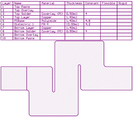
In order to make a rigid-flex board, different stacks in different areas need to be provided and clearly marked. A simple way is to copy the outline of the board on the mechanical layer, mark the areas where different layer stacks exist, and place the corresponding layer structure table next to it. If a 3D image showing the flexible and rigid areas can be generated, this will help manufacturers understand our intentions more clearly. Many people currently use MCAD software to achieve this view. They import the STEP file of the PCB design into the MCAD software.
So the Stack file is a very important file which could give us Juniper Flex PCB manufacturer a clear understanding of your designs and good to the manufacturing process.
4. Defining the Drill
Drill hole placement in rigid-flex PCBs is a complex task that requires precise control to maintain electrical and mechanical integrity across multiple layers. Once you have specified where each component will go on the board, create a drill map detailing where each component type needs to be drilled on the board surface. This will allow you to optimize the drilling process by ensuring the holes are appropriately spaced so that they do not overlap or overlap any other features on the board.
Drill holes must be placed accurately in each layer of the PCB, considering both functional and mechanical needs. Proper drilling ensures the reliability of interconnections between layers.
Drilling for vias, mounting holes, and other components requires an understanding of layer-specific requirements. For example, drill diameters and positions in flexible areas must accommodate the bending without causing damage, while holes in rigid areas must ensure structural integrity. Precise drilling and placement are critical for the PCB’s longevity and functionality.
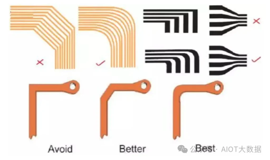
5. Circuit Routing Design
If there are traces on different layers in the flex area, try to avoid having one trace on the top layer and another trace on the bottom layer. This will cause inconsistent forces on the trace copper sheets on the upper and lower layers when the flex board is bent, which can easily cause mechanical damage to the line. Instead, the traces should be staggered and the paths should be arranged crosswise.
The design of the routing in the flex area requires arcs rather than angles. This is the opposite of the recommendations for the rigid area. This can protect the flexible board from being damaged when it is bent. The lines should also avoid sudden expansion or contraction, and teardrop-shaped arcs should be used to connect thick and thin lines.
6. Thermal Management and Reliability
Thermal management is a key challenge in rigid-flex PCB design. Proper heat dissipation techniques must be integrated to maintain reliable performance in temperature-sensitive applications.
Rigid-flex PCBs can generate significant heat, and without adequate thermal management, reliability may be compromised. Techniques like heat sinks and thermal vias help dissipate heat effectively.
By incorporating thermal vias, heat sinks, or thermal pads, you can effectively manage heat distribution across the PCB. It’s essential to analyze the heat generation patterns in both rigid and flexible sections of the PCB to prevent overheating and ensure long-term reliability.
7. Manufacturing and Assembly Considerations
The manufacturing and assembly process for rigid-flex PCBs is more complex than for traditional rigid or flexible boards, requiring special considerations for handling and assembly.
Precision in manufacturing processes is crucial to ensure that the flexible and rigid sections of the PCB are joined securely, without damaging sensitive areas.
Manufacturing rigid-flex PCBs requires specialized equipment and techniques, particularly for handling the flexible parts of the board during the soldering process. Assembly must be done carefully to avoid damaging the flex areas, which are more vulnerable to stress and heat than rigid areas.
Summary
Currently, miniaturization is the general trend, electronic products and components are becoming smaller and smaller, and PCBs (printed circuit boards) are becoming more compact. The challenges will become greater. So good designing at the beginning is very important for rigid-flex PCBs’ customers and manufacturers. By following design guidelines and carefully planning each step, you can create reliable and high-performance PCBs.
Juniper FPC also provide your the technical support from the design to rigid-flex PCB manufacturing. Welcome to talk about your rigid-flex PCB projects with our rigid-flex PCB exports.